
【CG】GPU硬件架构及运行机制
本文目录 40 个章节
【CG】GPU硬件架构及运行机制
创建时间:2020/11/26 16:27
- 【CG】GPU硬件架构及运行机制
- GPU Overview
- 特性与功能
- Stream processing
- 相关概念
- 显卡(Video card、Display card、Graphics card)
- Die (integrated circuit)
- CUDA
- 特性与功能
- CPU vs. GPU
- CPU - 擅长逻辑控制和串行的运算
- GPU - 适用于计算密集型和易于并发的程序
- GPU Architecture
- 术语
- Architecture
- The logical pipeline
- GPU资源机制
- 内存架构
- CPU-GPU异构系统
- CPU-GPU数据流
- GPU资源管理模型
- GPU Context
- GPU Channel
- 显像机制
- 单缓冲
- 双缓冲
- 垂直同步
- GPU技术要点
- SIMD和SIMT
- co-issue
- Early-Z
- 统一着色器架构(Unified shader Architecture)
- 渲染优化建议
- 减少CPU和GPU的数据交换
- 减少过绘制
- Shader优化
- GPU相关参数
- 其他相关知识
- GPU厂商及历史
- N卡历史
- NVIDIA GPU架构发展史
- GPU厂商及历史
- Ref
- GPU Overview
GPU Overview
GPU(Graphics Processing Unit,图形处理单元) - A graphics processing unit (GPU) is a specialized, electronic circuit designed to rapidly manipulate and alter memory to accelerate the creation of images in a frame buffer intended for output to a display device.
特性与功能
Modern GPUs are very efficient at manipulating computer graphics and image processing. Their highly parallel structure makes them more efficient than general-purpose central processing units (CPUs) for algorithms that process large blocks of data in parallel.
渲染图形
物理模拟
(海量)数学计算
AI运算
音视频编解码、加解密、科学计算、离线渲染等等都离不开现代GPU的并行计算能力和海量吞吐能力。
Stream processing
GPUs can only process independent vertices and fragments, but can process many of them in parallel. This is especially effective when the programmer wants to process many vertices or fragments in the same way. In this sense, GPUs are stream processors – processors that can operate in parallel by running one kernel on many records in a stream at once.
A stream is simply a set of records that require similar computation. Streams provide data parallelism.
Kernels are the functions that are applied to each element in the stream.
In the GPUs, vertices and fragments are the elements in streams and vertex and fragment shaders are the kernels to be run on them. For each element we can only read from the input, perform operations on it, and write to the output. It is permissible to have multiple inputs and multiple outputs, but never a piece of memory that is both readable and writable.
相关概念
显卡(Video card、Display card、Graphics card)
显卡上有:GPU、扇热器、通讯元件、与主板和显示器连接的各类插槽。 GPU是显卡最核心的部件。
Die (integrated circuit)
A die, in the context of integrated circuits, is a small block of semiconducting material on which a given functional circuit is fabricated.
CUDA
CUDA (Compute Unified Device Architecture) is a parallel computing platform and application programming interface (API) model created by Nvidia.
CPU vs. GPU
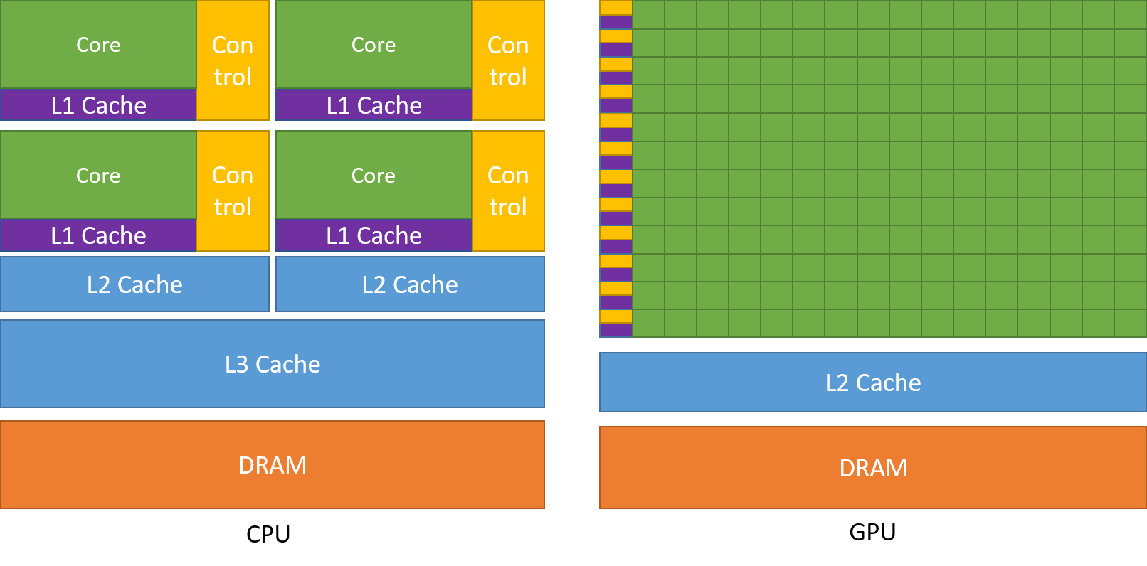
| property | CPU | GPU |
|---|---|---|
| compute density | Low | High |
| control logic | Complex | Simple |
| caches | Larger | Small |
| latency tolerance | Low | High |
| 并行目标 | 任务(Task) | 数据(Data) |
| 核心架构 | 多线程核心 | SIMT核心 |
| 线程数量级别 | 10 | 10000 |
| pipeline特点 | Shallow pipelines | Deep pipeline |
CPU - 擅长逻辑控制和串行的运算
CPU有很强大算术逻辑单元,减少操作延迟;巨大的cache,为了降低内存访问的延迟;复杂的控制器,使用分支预测来减少分支延迟,使用数据转发减少数据延迟。
GPU - 适用于计算密集型和易于并发的程序
GPU有小的cache,用来促进吞吐量;简单的控制,没有分支预测和数据转发;高效节能的ALU,很多延迟很长的ALU,但是为了高吞吐量被重度管线化;需要开启大量的线程才能降低延迟。
GPU Architecture
术语
GPCs(Graphics Processing Cluster)
TPC(Texture Processor Cluster,纹理处理簇)
SP(Streaming Processor,流处理器)
SM(Stream Multiprocessor,流多处理器)
SFU(Special Function Unit,特殊函数单元)
分发单元(Dispatch Unit)
加载存储单元(LD/ST)
Warp(线程束)
FPU( Float Point Unit,浮点运算单元)
ALU(Arithmetic Logical Unit,算术逻辑单元)
T&L(Transform & lighting,坐标变换和光照)
曲面细分(Tessellation)
外壳着色器(Hull Shader)
镶嵌单元(tessellator)
域着色器(Domain Shader)
Architecture
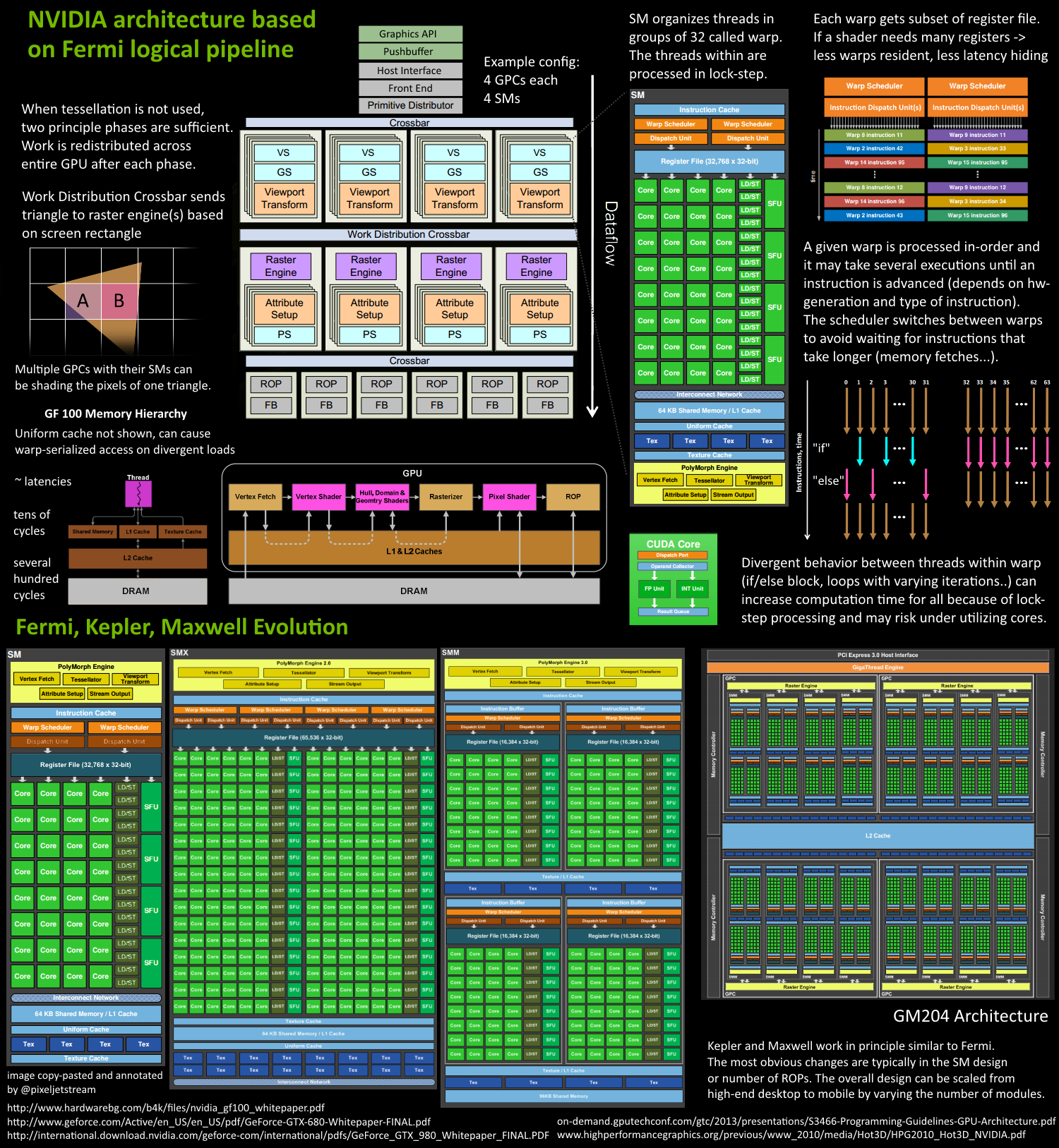
Since Fermi NVIDIA has a similar principle architecture.
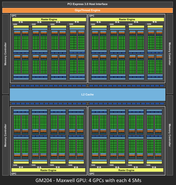
There is a Giga Thread Engine which manages all the work that’s going on. The GPU is partitioned into multiple GPCs (Graphics Processing Cluster), each has multiple SMs (Streaming Multiprocessor) and one Raster Engine. There is lots of interconnects in this process, most notably a Crossbar that allows work migration across GPCs or other functional units like ROP (render output unit) subsystems.
The work that a programmer thinks of (shader program execution) is done on the SMs. It contains many Cores which do the math operations for the threads. One thread could be a vertex-, or pixel-shader invocation for example. Those cores and other units are driven by Warp Schedulers , which manage a group of 32 threads as warp and hand over the instructions to be performed to Dispatch Units. The code logic is handled by the scheduler and not inside a core itself, which just sees something like “sum register 4234 with register 4235 and store in 4230” from the dispatcher.
总结: 1个GPU包括多个GPC 1个GPU包括多个SM 1个着色器程序由1个SM负责 1个SM包含多个Cores(如32个) 1个Core一次执行1个thread 1个thread可以是1个vertex-shader或pixel-shader的一次调用 1个Warp(线程束)为a group of 32 threads Warp Schedulers管理warp
GPU is a collection of stream processors. Each processor is capable of executing X threads simultaneously. Each processor runs 1 thread group(warp) at a time.
Blocks are divided into 32 thread wide units called warps
- Size of warps is implementation specific and can change in the future
The SM creates, manages, schedules and executes threads at warp granularity
- Each warp consists of 32 threads of contiguous threadIds
All threads in a warp execute the same instruction
- If threads of a warp diverge the warp serially executes each branch path taken
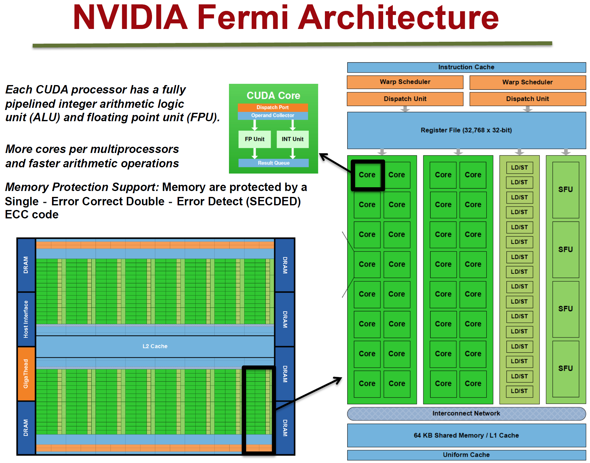
Fermi架构 Fermi was the first NVIDIA GPU implementing a fully scalable graphics engine and its core architecture can be found in Kepler as well as Maxwell.
拥有16个SM
每个SM:
2个Warp(线程束)
两组共32个Core
16组加载存储单元(LD/ST)
4个特殊函数单元(SFU)
每个Warp:
16个Core
Warp编排器(Warp Scheduler)
分发单元(Dispatch Unit)
每个Core:
1个FPU(浮点数单元)
1个ALU(逻辑运算单元)
The logical pipeline
摘自: https://developer.nvidia.com/content/life-triangle-nvidias-logical-pipeline
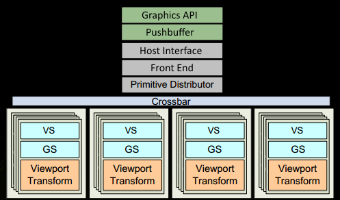
- The program makes a drawcall in the graphics api (DX or GL). This reaches the driver at some point which does a bit of validation to check if things are “legal” and inserts the command in a GPU-readable encoding inside a pushbuffer.
A lot of bottlenecks can happen here on the CPU side of things, which is why it is important programmers use apis well, and techniques that leverage the power of today’s GPUs.
After a while or explicit “flush” calls, the driver has buffered up enough work in a pushbuffer and sends it to be processed by the GPU (with some involvement of the OS). The Host Interface of the GPU picks up the commands which are processed via the Front End.
We start our work distribution in the Primitive Distributor by processing the indices in the indexbuffer and generating triangle work batches that we send out to multiple GPCs.
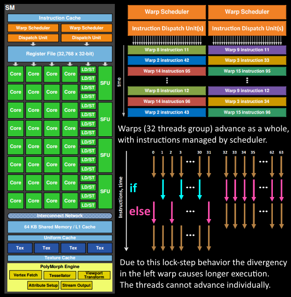
Within a GPC, the Poly Morph Engine of one of the SMs takes care of fetching the vertex data from the triangle indices (Vertex Fetch).
After the data has been fetched, warps of 32 threads are scheduled inside the SM and will be working on the vertices.
The SM’s warp scheduler issues the instructions for the entire warp in-order. The threads run each instruction in lock-step and can be masked out individually if they should not actively execute it. There can be multiple reasons for requiring such masking. For example when the current instruction is part of the “if (true)” branch and the thread specific data evaluated “false”, or when a loop’s termination criteria was reached in one thread but not another. Therefore having lots of branch divergence in a shader can increase the time spent for all threads in the warp significantly. Threads cannot advance individually, only as a warp! Warps, however, are independent of each other.
在一个warp中的分支除非32个线程都走到if或者else里面,否则相当于所有的分支都走了一遍
The warp’s instruction may be completed at once or may take several dispatch turns. For example the SM typically has less units for load/store than doing basic math operations.
As some instructions take longer to complete than others, especially memory loads, the warp scheduler may simply switch to another warp that is not waiting for memory. This is the key concept how GPUs overcome latency of memory reads, they simply switch out groups of active threads. To make this switching very fast, all threads managed by the scheduler have their own registers in the register-file. The more registers a shader program needs, the less threads/warps have space. The less warps we can switch between, the less useful work we can do while waiting for instructions to complete (foremost memory fetches).
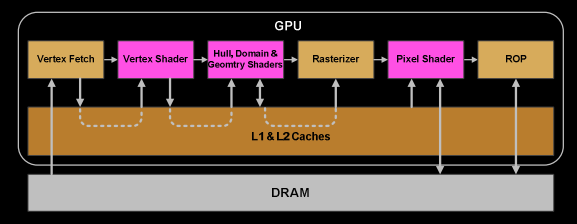
- Once the warp has completed all instructions of the vertex-shader, it’s results are being processed by Viewport Transform. The triangle gets clipped by the clipspace volume and is ready for rasterization. We use L1 and L2 Caches for all this cross-task communication data.
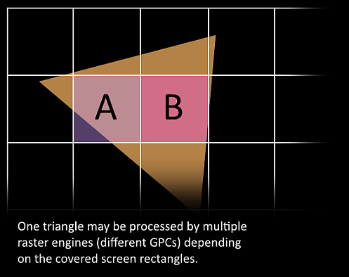
- Now it gets exciting, our triangle is about to be chopped up and potentially leaving the GPC it currently lives on. The bounding box of the triangle is used to decide which raster engines need to work on it, as each engine covers multiple tiles of the screen. It sends out the triangle to one or multiple GPCs via the Work Distribution Crossbar. We effectively split our triangle into lots of smaller jobs now.
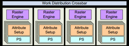
Attribute Setup at the target SM will ensure that the interpolants (for example the outputs we generated in a vertex-shader) are in a pixel shader friendly format.
The Raster Engine of a GPC works on the triangle it received and generates the pixel information for those sections that it is responsible for (also handles back-face culling and Z-cull).
Again we batch up 32 pixel threads, or better say 8 times 2x2 pixel quads, which is the smallest unit we will always work with in pixel shaders. This 2x2 quad allows us to calculate derivatives for things like texture mip map filtering (big change in texture coordinates within quad causes higher mip). Those threads within the 2x2 quad whose sample locations are not actually covering the triangle, are masked out (gl_HelperInvocation). One of the local SM’s warp scheduler will manage the pixel-shading task.
The same warp scheduler instruction game, that we had in the vertex-shader logical stage, is now performed on the pixel-shader threads. The lock-step processing is particularly handy because we can access the values within a pixel quad almost for free, as all threads are guaranteed to have their data computed up to the same instruction point.

- Almost, our pixel-shader has completed the calculation of the colors to be written to the rendertargets and we also have a depth value. At this point we have to take the original api ordering of triangles into account before we hand that data over to one of the ROP (render output unit) subsystems, which in itself has multiple ROP units. Here depth-testing, blending with the framebuffer and so on is performed. These operations need to happen atomically (one color/depth set at a time) to ensure we don’t have one triangle’s color and another triangle’s depth value when both cover the same pixel. NVIDIA typically applies memory compression, to reduce memory bandwidth requirements, which increases “effective” bandwidth .
Warp是典型的单指令多线程(SIMT,SIMD单指令多数据的升级)的实现,也就是32个线程同时执行的指令是一模一样的,只是线程数据不一样,这样的好处就是一个warp只需要一个套逻辑对指令进行解码和执行就可以了,芯片可以做的更小更快,之所以可以这么做是由于GPU需要处理的任务是天然并行的。
GPU资源机制
内存架构
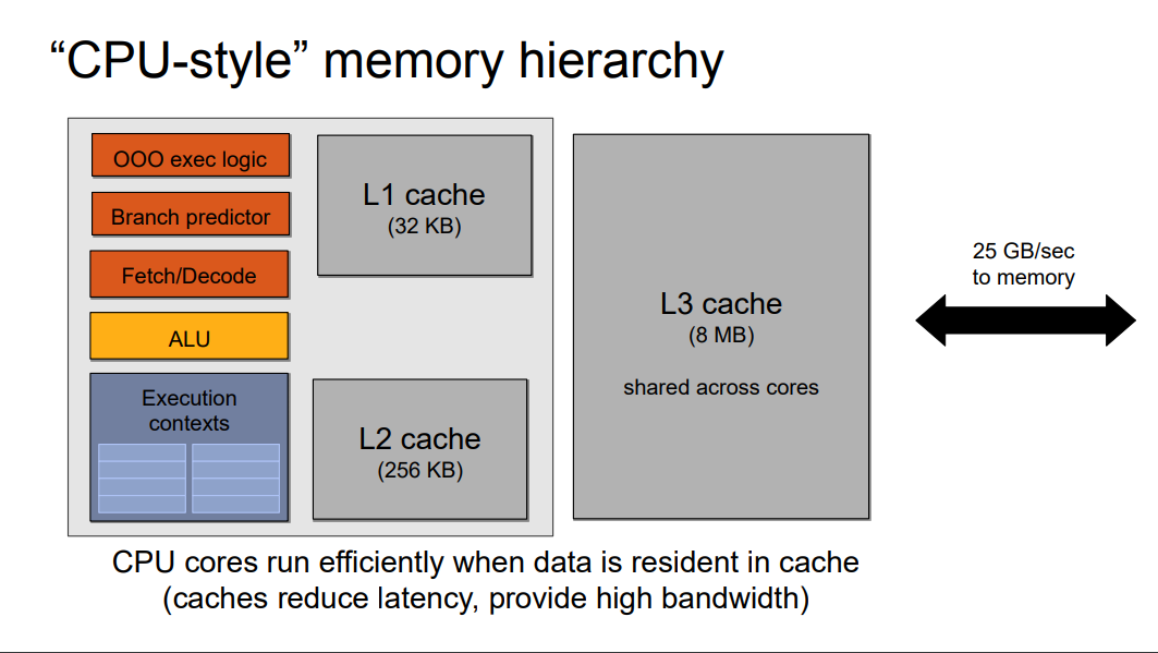
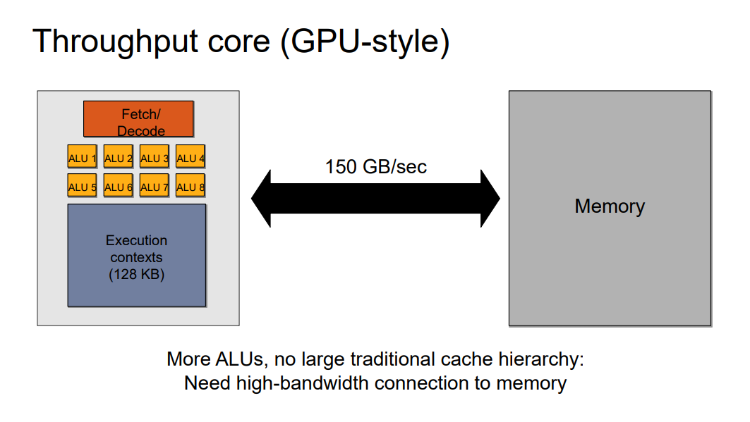
这种架构的特点是ALU多,GPU上下文(Context)多,吞吐量高,依赖高带宽与系统内存交换数据。
CPU-GPU异构系统
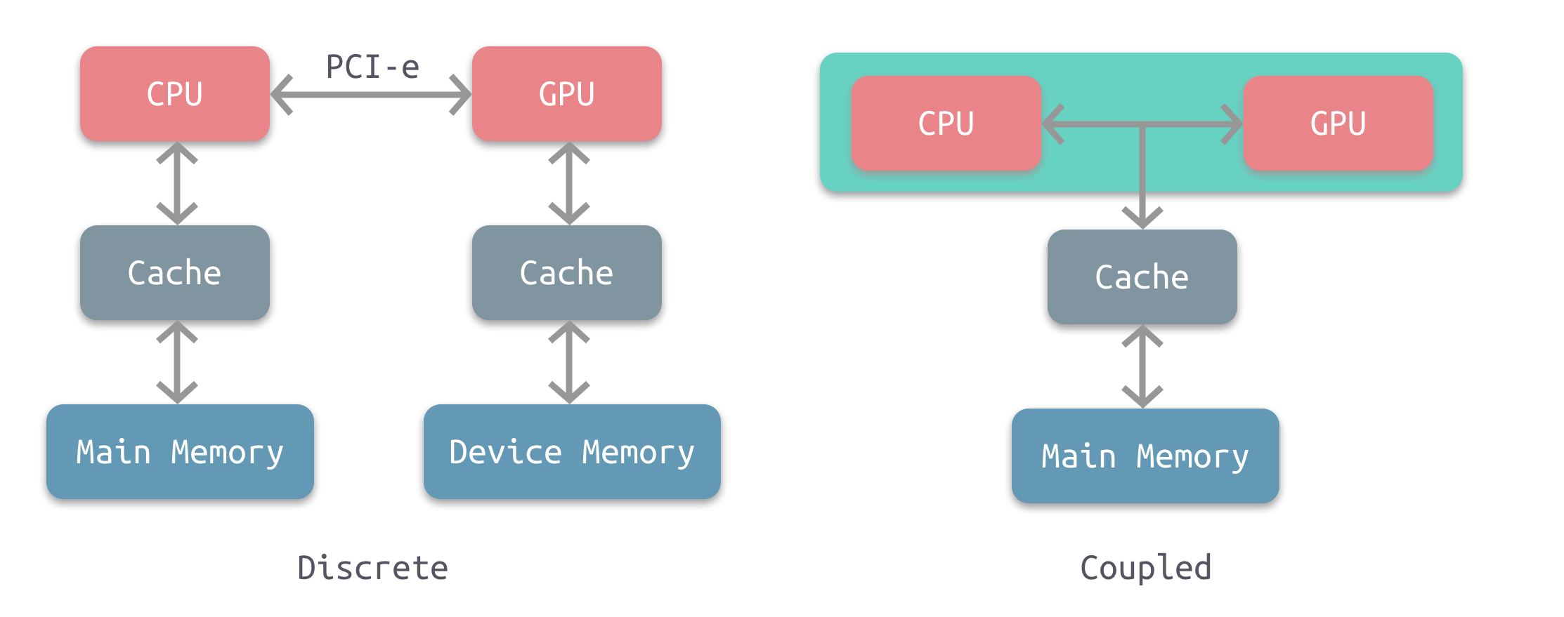
上图左是分离式架构,CPU和GPU各自有独立的缓存和内存,它们通过PCI-e等总线通讯。这种结构的缺点在于 PCI-e 相对于两者具有低带宽和高延迟,数据的传输成了其中的性能瓶颈。目前使用非常广泛,如PC、智能手机等。
上图右是耦合式架构,CPU 和 GPU 共享内存和缓存。AMD 的 APU 采用的就是这种结构,目前主要使用在游戏主机中,如 PS4。
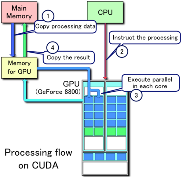
CPU-GPU数据流
分离式架构的CPU-GPU的数据流程图:
GPU资源管理模型
GPU Context
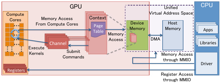
GPU Context代表了GPU计算的状态。
在GPU中拥有自己的虚拟地址。
GPU 中可以并存多个活跃态下的Context。
GPU Channel
任何命令都是由CPU发出。
命令流(command stream)被提交到硬件单元,也就是GPU Channel。
每个GPU Channel关联一个context,而一个GPU Context可以有多个GPU channel。
每个GPU Context 包含相关channel的 GPU Channel Descriptors , 每个 Descriptor 都是 GPU 内存中的一个对象。
每个 GPU Channel Descriptor 存储了 Channel 的设置,其中就包括 Page Table 。
每个 GPU Channel 在GPU内存中分配了唯一的命令缓存,这通过MMIO对CPU可见。
GPU Context Switching 和命令执行都在GPU硬件内部调度。
显像机制
单缓冲
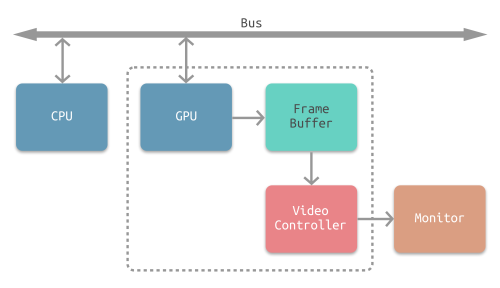
CPU将计算好显示内容提交至 GPU,GPU 渲染完成后将渲染结果存入帧缓冲区,视频控制器会按照 VSync 信号逐帧读取帧缓冲区的数据,经过数据转换后最终由显示器进行显示。
在早期的CRT显示器,电子枪从上到下逐行扫描,扫描完成后显示器就呈现一帧画面。然后电子枪回到初始位置进行下一次扫描。为了同步显示器的显示过程和系统的视频控制器,显示器会用硬件时钟产生一系列的定时信号。
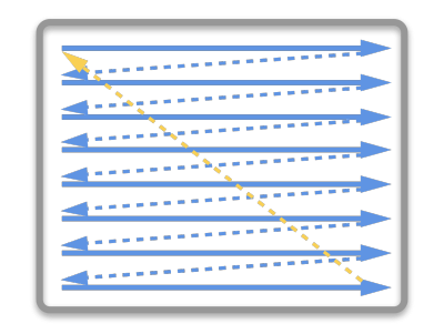
当电子枪换行进行扫描时,显示器会发出一个 水平同步信号 (horizonal synchronization),简称 HSync
当一帧画面绘制完成后,电子枪回复到原位,准备画下一帧前,显示器会发出一个 垂直同步信号 (vertical synchronization),简称 VSync。
显示器通常以固定频率进行刷新,这个刷新率就是 VSync 信号产生的频率。虽然现在的显示器基本都是液晶显示屏了,但其原理基本一致。
双缓冲
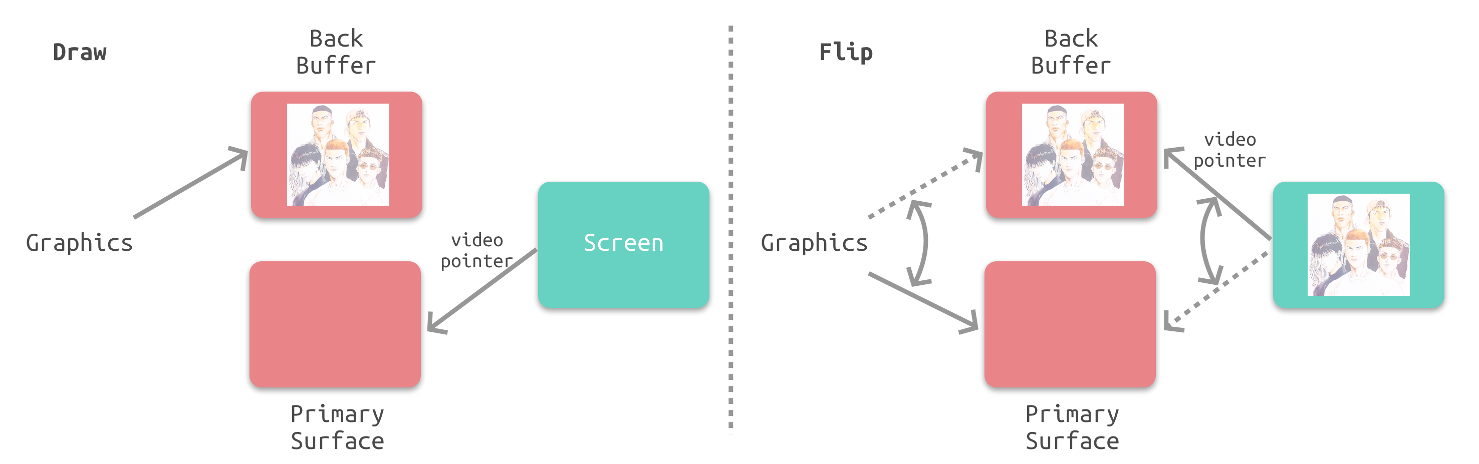
在单缓冲下,帧缓冲区的读取和刷新都都会有比较大的效率问题,经常会出现相互等待的情况,导致帧率下降。
为了解决效率问题,GPU 通常会引入两个缓冲区,即 双缓冲机制。在这种情况下,GPU 会预先渲染一帧放入一个缓冲区中,用于视频控制器的读取。当下一帧渲染完毕后,GPU 会直接把视频控制器的指针指向第二个缓冲器。
垂直同步
双缓冲虽然能解决效率问题,但会引入一个新的问题。当视频控制器还未读取完成时,即屏幕内容刚显示一半时,GPU 将新的一帧内容提交到帧缓冲区并把两个缓冲区进行交换后,视频控制器就会把新的一帧数据的下半段显示到屏幕上,造成画面撕裂现象:
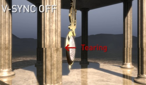
为了解决这个问题,GPU 通常有一个机制叫做垂直同步(简写也是V-Sync),当开启垂直同步后,GPU 会等待显示器的 VSync 信号发出后,才进行新的一帧渲染和缓冲区更新。这样能解决画面撕裂现象,也增加了画面流畅度,但需要消费更多的计算资源,也会带来部分延迟。
GPU技术要点
SIMD和SIMT
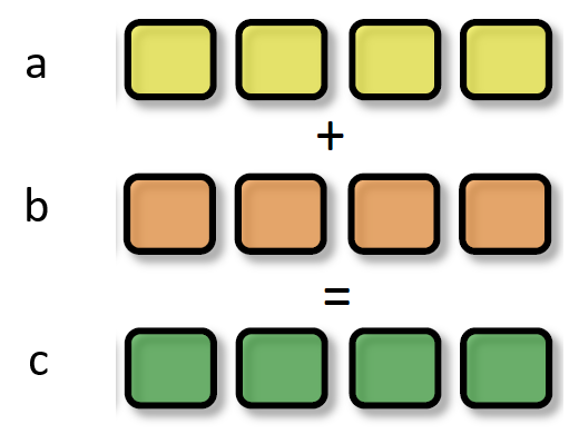
SIMD(Single Instruction Multiple Data)是单指令多数据,在GPU的ALU单元内,一条指令可以处理多维向量(一般是4D)的数据。
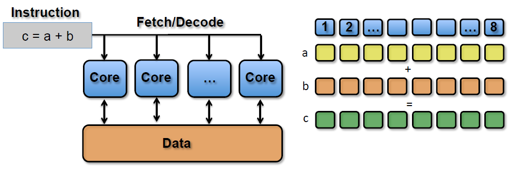
SIMT(Single Instruction Multiple Threads,单指令多线程)是SIMD的升级版,可对GPU中单个SM中的多个Core同时处理同一指令,并且每个Core存取的数据可以是不同的。
co-issue
co-issue是为了解决SIMD运算单元无法充分利用的问题。
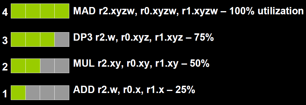
为了解决着色器在低维向量的利用率低的问题,可以通过合并1D与3D或2D与2D的指令。 于是 标量指令着色器(Scalar Instruction Shader) 应运而生,它可以有效地组合任何向量,开启co-issue技术,充分发挥SIMD的优势。
Early-Z

Early-Z技术可以将很多无效的像素提前剔除,避免它们进入耗时严重的像素着色器。Early-Z剔除的最小单位不是1像素,而是像素块(pixel quad,2x2个像素 以下情况会导致Early-Z失效:
开启Alpha Test:由于Alpha Test需要在像素着色器后面的Alpha Test阶段比较,所以无法在像素着色器之前就决定该像素是否被剔除。
开启Alpha Blend:启用了Alpha混合的像素很多需要与frame buffer做混合,无法执行深度测试,也就无法利用Early-Z技术。
开启Tex Kill:即在shader代码中有像素摒弃指令(DX的discard,OpenGL的clip)。
关闭深度测试。Early-Z是建立在深度测试看开启的条件下,如果关闭了深度测试,也就无法启用Early-Z技术。
开启Multi-Sampling:多采样会影响周边像素,而Early-Z阶段无法得知周边像素是否被裁剪,故无法提前剔除。
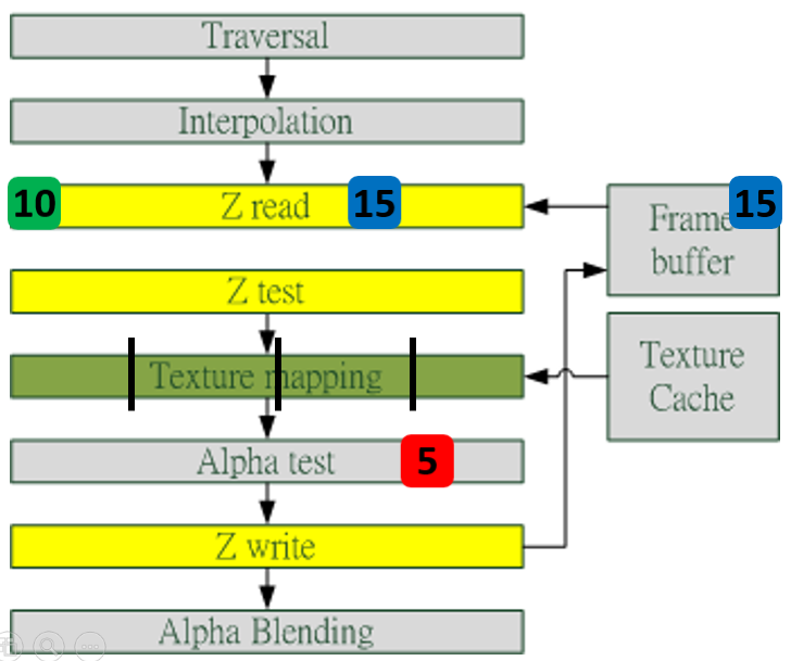
Early-Z技术会导致一个问题:深度数据冲突(depth data hazard)。 假设数值深度值5已经经过Early-Z即将写入Frame Buffer,而深度值10刚好处于Early-Z阶段,读取并对比当前缓存的深度值15,结果就是10通过了Early-Z测试,会覆盖掉比自己小的深度值5,最终frame buffer的深度值是错误的结果。
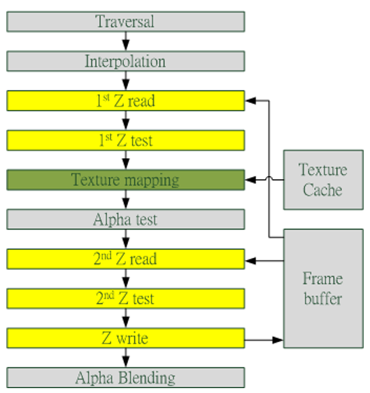
避免深度数据冲突的方法之一是在写入深度值之前,再次与frame buffer的值进行对比:
统一着色器架构(Unified shader Architecture)
在早期的GPU,顶点着色器和像素着色器的硬件结构是独立的,它们各有各的寄存器、运算单元等部件。这样很多时候,会造成顶点着色器与像素着色器之间任务的不平衡。对于顶点数量多的任务,像素着色器空闲状态多;对于像素多的任务,顶点着色器的空闲状态多。
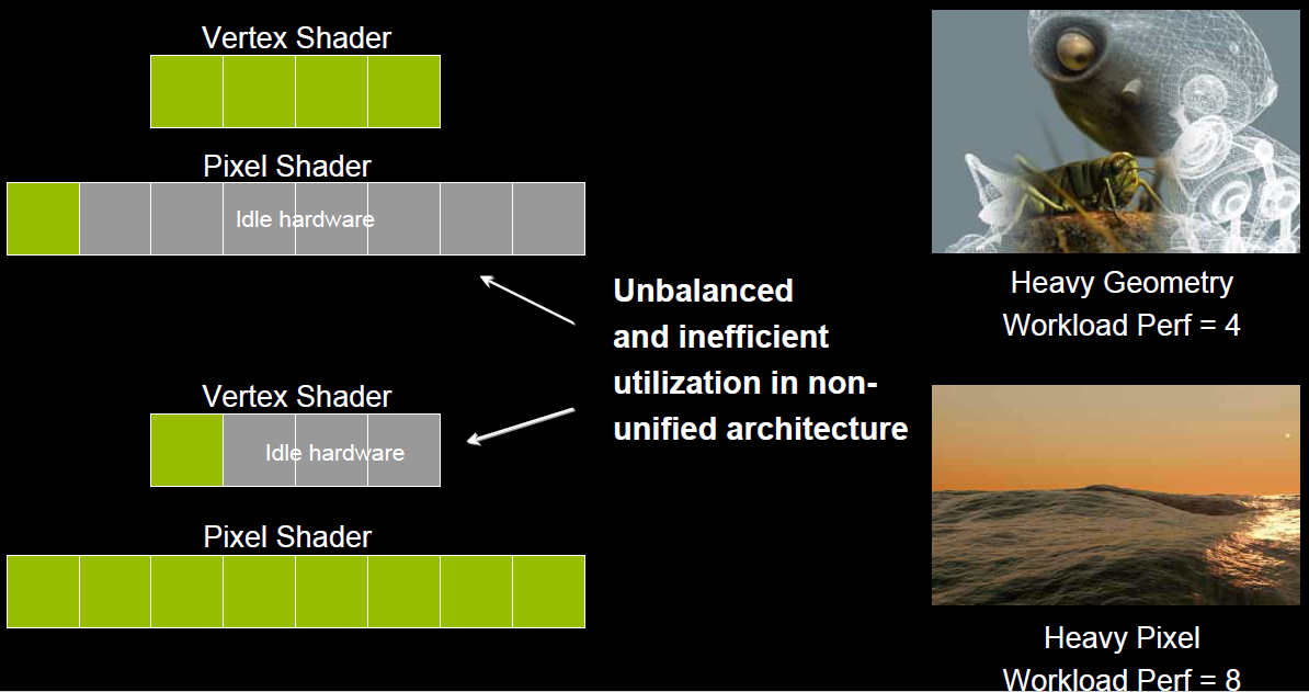
于是,为了解决VS和PS之间的不平衡,引入了统一着色器架构(Unified shader Architecture)。用了此架构的GPU,VS和PS用的都是相同的Core。也就是,同一个Core既可以是VS又可以是PS。
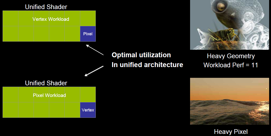
这样就解决了不同类型着色器之间的不平衡问题,还可以减少GPU的硬件单元,压缩物理尺寸和耗电量。此外,VS、PS可还可以和其它着色器(几何、曲面、计算)统一为一体。
渲染优化建议
减少CPU和GPU的数据交换
合批(Batch)
减少顶点数、三角形数
视锥裁剪
BVH
Portal
BSP
OSP
避免每帧提交Buffer数据
- CPU版的粒子、动画会每帧修改、提交数据,可移至GPU端。
减少渲染状态设置和查询
例如:glGetUniformLocation会从GPU内存查询状态,耗费很多时间周期。
避免每帧设置、查询渲染状态,可在初始化时缓存状态。
启用GPU Instance
开启LOD
避免从显存读数据
减少过绘制
避免Tex Kill操作
避免Alpha Test
避免Alpha Blend
开启深度测试
Early-Z
层次Z缓冲(Hierarchical Z-Buffering,HZB)
开启裁剪:
背面裁剪
遮挡裁剪
视口裁剪
剪切矩形(scissor rectangle)
控制物体数量
粒子数量多且面积小,由于像素块机制,会加剧过绘制情况
植物、沙石、毛发等也如此
Shader优化
避免if、switch分支语句
避免for循环语句,特别是循环次数可变的
减少纹理采样次数
禁用clip或discard操作
减少复杂数学函数调用
GPU相关参数
GFLOPS 就是 Giga FLoating-point Operations Per Second,即每秒10亿次的浮点运算数。
其他相关知识
GPU厂商及历史
NVIDIA - N卡。代表产品有GeForce系列、GTX系列、RTX系列等。
AMD/ATI - 既是CPU生产商,也是GPU生产商。A卡。代表产品有Radeon系列。
In 2009, Intel, Nvidia and AMD/ATI were the market share leaders, with 49.4%, 27.8% and 20.6% market share respectively. However, those numbers include Intel’s integrated graphics solutions as GPUs. Not counting those, Nvidia and AMD control nearly 100% of the market as of 2018. Their respective market shares are 66% and 33%. In addition, S3 Graphics[64] and Matrox produce GPUs. Modern smartphones also use mostly Adreno GPUs from Qualcomm, PowerVR GPUs from Imagination Technologies and Mali GPUs from ARM.
N卡历史
1995 – NV1
1997 – Riva 128 (NV3), DX3
1998 – Riva TNT (NV4), DX5 32位颜色, 24位Z缓存, 8位模板缓存 双纹理, 双线性过滤 每时钟2像素 (2 ppc)
1999 - GeForce 256(NV10) 固定管线,支持DirectX 7.0 硬件T&L(Transform & lighting,坐标变换和光照) 立方体环境图(Cubemaps) DOT3 – bump mapping 2倍各向异性过滤 三线性过滤 DXT纹理压缩 4ppc 引入“GPU”术语
2001 - GeForce 3 DirectX 8.0 Shader Model 1.0 可编程渲染管线 顶点着色器 像素着色器 3D纹理 硬件阴影图 8倍各向异性过滤 多采样抗锯齿(MSAA) 4 ppc
2003 - GeForce FX系列(NV3x) DirectX 9.0 Shader Model 2.0 256顶点操作指令 32纹理 + 64算术像素操作指令 Shader Model 2.0a 256顶点操作指令 512像素操作指令 着色语言 - HLSL CGSL GLSL
2004 - GeForce 6系列 (NV4x) DirectX 9.0c Shader Model 3.0 动态流控制 分支、循环、声明等 顶点纹理读取 高动态范围(HDR) 64位渲染纹理(Render Target) FP16*4 纹理过滤和混合
2006 - GeForce 8系列 (G8x) DirectX 10.0 Shader Model 4.0 几何着色器(Geometry Shaders) 没有上限位(No caps bits) 统一的着色器(Unified Shaders) Vista系统全新驱动 基于GPU计算的CUDA问世 GPU计算能力以GFLOPS计量。
2010 - GeForce 405(GF119) DirectX 11.0 曲面细分(Tessellation) 外壳着色器(Hull Shader) 镶嵌单元(tessellator) 域着色器(Domain Shader) 计算着色器(Compute Shader) 支持Stream Output DirectX 11的渲染管线。 多线程支持 改进的纹理压缩 Shader Model 5.0 更多指令、存储单元、寄存器 面向对象着色语言 曲面细分 计算着色器
2014 - GeForceGT 710(GK208) DirectX 12.0 轻量化驱动层 硬件级多线程渲染支持 更完善的硬件资源管理
2016 - GeForceGTX 1060 6GB 首次支持RTX和DXR技术,即支持光线追踪 引入RT Core(光线追踪核心) 支持RTX光线追踪的显卡列表。
2018 - TITAN RTX(TU102) DirectX 12.1,OpenGL 4.5 6GPC,36TPC,72SM,72RT Core,… 8K分辨率,1770MHz主频,24G显存,384位带宽
NVIDIA GPU架构发展史
2008 - Tesla Tesla最初是给计算处理单元使用的,应用于早期的CUDA系列显卡芯片中,并不是真正意义上的普通图形处理芯片。
2010 - Fermi Fermi是第一个完整的GPU计算架构。首款可支持与共享存储结合纯cache层次的GPU架构,支持ECC的GPU架构。
2012 - Kepler Kepler相较于Fermi更快,效率更高,性能更好。
2014 - Maxwell 其全新的立体像素全局光照 (VXGI) 技术首次让游戏 GPU 能够提供实时的动态全局光照效果。基于 Maxwell 架构的 GTX 980 和 970 GPU 采用了包括多帧采样抗锯齿 (MFAA)、动态超级分辨率 (DSR)、VR Direct 以及超节能设计在内的一系列新技术。
2016 - Pascal Pascal 架构将处理器和数据集成在同一个程序包内,以实现更高的计算效率。1080系列、1060系列基于Pascal架构
2017 - Volta Volta 配备640 个Tensor 核心,每秒可提供超过100 兆次浮点运算(TFLOPS) 的深度学习效能,比前一代的Pascal 架构快5 倍以上。
2018 - Turing Turing 架构配备了名为 RT Core 的专用光线追踪处理器,能够以高达每秒 10 Giga Rays 的速度对光线和声音在 3D 环境中的传播进行加速计算。Turing 架构将实时光线追踪运算加速至上一代 NVIDIA Pascal™ 架构的 25 倍,并能以高出 CPU 30 多倍的速度进行电影效果的最终帧渲染。2060系列、2080系列显卡也是跳过了Volta直接选择了Turing架构。
Ref
https://www.cnblogs.com/timlly/p/11471507.html https://en.wikipedia.org/wiki/Graphics_processing_unit https://sites.google.com/site/daveshshingari/explorations/computer-architecture/gpu-architecture NVIDIA’s logical pipeline: https://developer.nvidia.com/content/life-triangle-nvidias-logical-pipeline http://haifux.org/lectures/267/Introduction-to-GPUs.pdf http://people.cs.pitt.edu/~melhem/courses/3580p/gpu.pdf https://i.dell.com/sites/csdocuments/Shared-Content_data-Sheets_Documents/en/NVIDIA-Fermi-Compute-Architecture-Whitepaper-en.pdf https://zhuanlan.zhihu.com/p/53785954